Variable frequency drive Rectifier
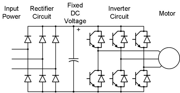
To understand variable frequency drive (VFD) better, it's necessary to explain some of the main parts of the variable frequency drive. The main two parts of a VFD are the rectifier and the inverter. The first will convert the AC voltage into a DC voltage; the second will convert this DC voltage into an AC voltage with variable magnitude and frequency. So together they form an AC to AC converter tool which can be placed between the normal electric grid and a load with a special demand for voltage and frequency characteristics.
The most common used variable frequency drive components to rectify AC voltage to DC voltage are ordinary semiconducting diodes. This is done for several reasons. First these diodes are basically just what is needed because they conduct the current in one direction and block it in the other direction. The AC voltage becomes positively or negatively rectified. Actually, it is the current which is rectified. To make the voltage also rectified capacitors are needed in addition. A second reason for the use of diodes as the basic components of the rectifier in variable frequency drive is the low price compared with other semiconducting technologies. The diode is also far more robust than other (steered) semiconductors. A third reason which makes the choice for diodes logic is the absent of control electronics to bring the diode in or out conduction. The commutation process happens naturally so the control is not needed. Because of the use of diodes, several suppositions can be made:
One phase rectifier
1. Current course
The diode in Figure 1 is comparable with a switch which is closed at t = 0 (Figure 2). The formula for the current is then:

Fig.1 One phase half wave rectifier

Fig. 2 (a) Switch as equivalent of the diode; (b) Current course switch
The inductance will oppose the cause of the changing magnetic field, namely the increasing current, by inducing a voltage with opposite potential compared with the source voltage. This reduces the current which can flow in the circuit of the vfd. So the current will not follow a course proportional with the voltage but will instead lag. Unlike an ordinary switch, the diode cannot conduct the current in the negative direction. When the current becomes zero, natural commutation occurs and the current becomes zero. The whole voltage is fixed over the diode. The current is rectified and by that, the voltage over the resistance also. The time that the diode conducts depends on the ratio between the inductive and resistive impedance. With a combination of inductance and resistor this time lays between fifty and hundred percent of the period of the variable frequency drive input voltage source. After this period the same cycle happens again.
2. Voltage course
The assumption is made that there is no voltage drop over the diode when it conducts. By this the following formula is always valid:

Fig. 3 Current and voltage course one phase rectifier over one period
From 0 to tm the inductance is loaded with energy:

Fig. 4 Curve of β for different values of φ
Three phase half-wave rectification
The principle of the variable frequency drive three phase half-wave rectification is capturing the positive or negative peaks of the three phase voltages by means of three diodes. The phase voltage is the potential between the neutral point and one of the phase wires. The rectifying circuit is build like showed in Figure 5. The two graphs give the three phase voltages and the output voltage. Both graphs start with positive alternation of phase voltage u1. From time t1 the voltage u1 is the highest what gives that diode D1 will conduct. When D1 conducts, the potential at the cathodes of both the other diodes D2 and D3 will reach the same potential as u1. So they block. At time t2 the voltage u2 becomes higher and from that moment on diode D2 will start conducting so that the cathode of D1 reaches the same potential as u2 and blocks. The same process happens with voltage u3 and diode D3. When the rectifying circuit is connected (here through a transformer) with the electric grid, the phase order of the grid will determine when which diode conducts or blocks.

Fig. 5 Circuit and wave pattern of a three phase half wave rectifier
An important process is the transition between the conducting states of the different diodes. This is called commutation. Because the rectifying circuits consist of simple diodes, the commutation will happen natural. Because there is always some kind of inductance in the circuit, the commutation process will never happen immediately. In the used example the leak inductance of the transformer prevents the sudden change in current through the diode, from conducting state to blocking state or vice versa. In Figure 5 at time t2 the current through D1 will still flow when D2 starts conducting. At that moment phases u1 and u2 will be sho1rt circuited. The short circuit voltage at the cathodes of both diodes is given by following formula:

Fig. 6 Actual waveforms in rectifier due to commutation between diodes
The next important factor that can be derived is the average direct current component of the vfd rectified voltage Uai. This can be done by use of Figure 7. In this graph, the origin is chosen so that phase voltage u1 reaches its maximum at time zero.

Fig. 7 Ripple on the output rectified voltage
By that following formula is applicable to describe the course of the phase voltage:
Three phase bridge rectification
The variable frequency drive three phase bridge rectifier uses six instead of three diodes like the three phase half-wave rectifier. In theory it is possible to connect the diode circuit directly on the grid but often a transformer is used between grid and diode bridge. This allows a transformation to another voltage and it gives a galvanic separation. The mounting of the diodes is illustrated in Figure 8.

Fig. 8 Three phase bridge rectifier separated from the grid by a transformer
The next important difference between the half-wave and bridge rectifier is the use of line voltage respectively phase voltage. In Figure 8 the letters L1, L2 and L3 give an indication of the three line wires. Between those wires three AC voltages are present with a phase shift of 120°. These are the line voltages. The indicating voltages u12, u23 and u31 refer to the potential between the line wire indicated by the first suffix number and the line wire indicated by the second suffix number. For instance: if u12 is positive that means that the phase voltage u1 is higher than the phase voltage u2 and by that the potential of line wire L1 is higher than the potential of line wire L2, Looking at the diode circuit of Figure 8 it is easily to see that at every moment the highest line voltage (positive or negative) stands over the vfd load. Hereby we can define line voltages u21, u32 and u13 by negating line voltages u12, u23 and u31, This line voltages answer also to the earlier given potential definition. In Figure 9 the sequence of the line voltages over the lo·ad is given. When u12 is the highest voltage, that means from the moment that u2 is maximal and negative until the moment that u1 is maximal and positive, the potential over the load is equal to u12, To close the circuit diodes D1 and D6 must conduct and the other diodes block. The following phase voltage is u13, From the moment that u1 is maximal and positive until the moment that u3 is maximal and negative u13 is the potential over the load and diodes D1 and D2 conduct. The following voltages over the load are found analogous. The diodes are numbered to make the sequence 1-2, 2-3, 3-4, 4-5, 5-6 and 6-1 where after the sequence restarts.

Fig. 9 Output voltage waveform and conducting diodes sequence
There are 6 diodes and the current has to be passed when they change from conducting state to blocking state or vice versa. Thus here acts the commutation principle. In points 1 to 6 there is commutation. In this circuit the commutation acts naturally. There conducts always one diode from the upper bridge half and one diode from the lower bridge half. If the voltage loss over diodes and during commutation is neglected, the output voltage is formed by the peak values of the line voltages. The output current follows the same course because the resistive load and Ohms law. This course isn't flat. It has a ripple. The frequency and magnitude of this ripple are important characteristics to differentiate different rectifiers. The pulse number is defined as:
Rectifier
The most common used variable frequency drive components to rectify AC voltage to DC voltage are ordinary semiconducting diodes. This is done for several reasons. First these diodes are basically just what is needed because they conduct the current in one direction and block it in the other direction. The AC voltage becomes positively or negatively rectified. Actually, it is the current which is rectified. To make the voltage also rectified capacitors are needed in addition. A second reason for the use of diodes as the basic components of the rectifier in variable frequency drive is the low price compared with other semiconducting technologies. The diode is also far more robust than other (steered) semiconductors. A third reason which makes the choice for diodes logic is the absent of control electronics to bring the diode in or out conduction. The commutation process happens naturally so the control is not needed. Because of the use of diodes, several suppositions can be made:
- Diodes act like switches without leakage current or voltage drop
- The switching occurs without time delay
- Assume a perfect three phase sinusoidal input voltage
- Assume a constant output current
One phase rectifier
1. Current course
The diode in Figure 1 is comparable with a switch which is closed at t = 0 (Figure 2). The formula for the current is then:
With:
The current i(t) has a course like drawn in Figure 3 (a). This figure gives two important characteristics of the diode in the circuit. Like a closing switch the current will show a transition phenomenon. When the voltage becomes positive the current will be also zero because of the inductance in the circuit.

Fig.1 One phase half wave rectifier
Fig. 2 (a) Switch as equivalent of the diode; (b) Current course switch
The inductance will oppose the cause of the changing magnetic field, namely the increasing current, by inducing a voltage with opposite potential compared with the source voltage. This reduces the current which can flow in the circuit of the vfd. So the current will not follow a course proportional with the voltage but will instead lag. Unlike an ordinary switch, the diode cannot conduct the current in the negative direction. When the current becomes zero, natural commutation occurs and the current becomes zero. The whole voltage is fixed over the diode. The current is rectified and by that, the voltage over the resistance also. The time that the diode conducts depends on the ratio between the inductive and resistive impedance. With a combination of inductance and resistor this time lays between fifty and hundred percent of the period of the variable frequency drive input voltage source. After this period the same cycle happens again.
2. Voltage course
The assumption is made that there is no voltage drop over the diode when it conducts. By this the following formula is always valid:
u = uLl + uRlwith:
uRl = i x RlIn Figure 3 (a) the current course is given for one period. (T = 2π) The maximal current imax is reached at time tm. From equation klk we can see that the voltage over the resistor uRl has the same shape. Because the load (inductance and resistor) receives the whole sine voltage, for every moment between 0 and t2 next formula is applicable:
uLl = u - uRlFrom 0 to tm the current increases and the voltage over the inductance is positive. From tm to t2 the current decreases to zero and the inductance induces a negative voltage. A pure inductance consumes no net energy during a whole period. This is valid here.
Fig. 3 Current and voltage course one phase rectifier over one period
From 0 to tm the inductance is loaded with energy:
W = ½Ll x imax2Both voltage over and current through the inductor have same sign. Between time tm and t2 this stored energy is released back to the resistor in the circuit. The current is positive and the voltage over the inductance turns negative. The energy flow is again:
W = ½Ll x imax2At time t2 all the energy in the inductance flowed back into the circuit. The third graph in Figure 3 gives the voltage over the inductance. When next two integrals are added, the sum is zero.
This has to be because φ is the magnetic flux of the inductance due to the changing current and the net flux after one period has to be zero. This is an important characteristic of an ideal inductance and is called the equal area criterion. The average voltage is by that also zero. The vfd average output voltage, which is upon using the equal area criterion equal to the average voltage over the resistor, can be derived as a function of the conduction angle.
The expression uai is used because it is the average value (suffix a) and it is the idealized situation where the rectifier is considered to have no losses (suffix i). The average output current becomes then:
Ig = Ugi/RlTo know the value of the conduction angle β next formula can be applied:
This can only be solved by iteration. This is done in Figure 4.
Fig. 4 Curve of β for different values of φ
Three phase half-wave rectification
The principle of the variable frequency drive three phase half-wave rectification is capturing the positive or negative peaks of the three phase voltages by means of three diodes. The phase voltage is the potential between the neutral point and one of the phase wires. The rectifying circuit is build like showed in Figure 5. The two graphs give the three phase voltages and the output voltage. Both graphs start with positive alternation of phase voltage u1. From time t1 the voltage u1 is the highest what gives that diode D1 will conduct. When D1 conducts, the potential at the cathodes of both the other diodes D2 and D3 will reach the same potential as u1. So they block. At time t2 the voltage u2 becomes higher and from that moment on diode D2 will start conducting so that the cathode of D1 reaches the same potential as u2 and blocks. The same process happens with voltage u3 and diode D3. When the rectifying circuit is connected (here through a transformer) with the electric grid, the phase order of the grid will determine when which diode conducts or blocks.
Fig. 5 Circuit and wave pattern of a three phase half wave rectifier
An important process is the transition between the conducting states of the different diodes. This is called commutation. Because the rectifying circuits consist of simple diodes, the commutation will happen natural. Because there is always some kind of inductance in the circuit, the commutation process will never happen immediately. In the used example the leak inductance of the transformer prevents the sudden change in current through the diode, from conducting state to blocking state or vice versa. In Figure 5 at time t2 the current through D1 will still flow when D2 starts conducting. At that moment phases u1 and u2 will be sho1rt circuited. The short circuit voltage at the cathodes of both diodes is given by following formula:
uc = (u1 + u2) / 2After t2 voltage u1 becomes less and voltage u2 more positive so that id1 decreases and id2 increases. The time to completely conduct or block is determined by the inductances and the difference between uc and u2 respectively u1. A graph of this process is given below in Figure 6.
Fig. 6 Actual waveforms in rectifier due to commutation between diodes
The next important factor that can be derived is the average direct current component of the vfd rectified voltage Uai. This can be done by use of Figure 7. In this graph, the origin is chosen so that phase voltage u1 reaches its maximum at time zero.
Fig. 7 Ripple on the output rectified voltage
By that following formula is applicable to describe the course of the phase voltage:
u1 = û.cos wtNow the average direct current voltage component can easily been derived:
Because the input voltage is a sine wave! next expression for the average value is valid:

The output current has the same shape as the voltage so that the same expression is valid as in the one phase rectifier case:
Ig = Ugi / Rl
Three phase bridge rectification
The variable frequency drive three phase bridge rectifier uses six instead of three diodes like the three phase half-wave rectifier. In theory it is possible to connect the diode circuit directly on the grid but often a transformer is used between grid and diode bridge. This allows a transformation to another voltage and it gives a galvanic separation. The mounting of the diodes is illustrated in Figure 8.
Fig. 8 Three phase bridge rectifier separated from the grid by a transformer
The next important difference between the half-wave and bridge rectifier is the use of line voltage respectively phase voltage. In Figure 8 the letters L1, L2 and L3 give an indication of the three line wires. Between those wires three AC voltages are present with a phase shift of 120°. These are the line voltages. The indicating voltages u12, u23 and u31 refer to the potential between the line wire indicated by the first suffix number and the line wire indicated by the second suffix number. For instance: if u12 is positive that means that the phase voltage u1 is higher than the phase voltage u2 and by that the potential of line wire L1 is higher than the potential of line wire L2, Looking at the diode circuit of Figure 8 it is easily to see that at every moment the highest line voltage (positive or negative) stands over the vfd load. Hereby we can define line voltages u21, u32 and u13 by negating line voltages u12, u23 and u31, This line voltages answer also to the earlier given potential definition. In Figure 9 the sequence of the line voltages over the lo·ad is given. When u12 is the highest voltage, that means from the moment that u2 is maximal and negative until the moment that u1 is maximal and positive, the potential over the load is equal to u12, To close the circuit diodes D1 and D6 must conduct and the other diodes block. The following phase voltage is u13, From the moment that u1 is maximal and positive until the moment that u3 is maximal and negative u13 is the potential over the load and diodes D1 and D2 conduct. The following voltages over the load are found analogous. The diodes are numbered to make the sequence 1-2, 2-3, 3-4, 4-5, 5-6 and 6-1 where after the sequence restarts.
Fig. 9 Output voltage waveform and conducting diodes sequence
There are 6 diodes and the current has to be passed when they change from conducting state to blocking state or vice versa. Thus here acts the commutation principle. In points 1 to 6 there is commutation. In this circuit the commutation acts naturally. There conducts always one diode from the upper bridge half and one diode from the lower bridge half. If the voltage loss over diodes and during commutation is neglected, the output voltage is formed by the peak values of the line voltages. The output current follows the same course because the resistive load and Ohms law. This course isn't flat. It has a ripple. The frequency and magnitude of this ripple are important characteristics to differentiate different rectifiers. The pulse number is defined as:
p = frequency ripple / frequency sourceThe before described three phase half-wave rectifier has a pulse number of three and the three phase bridge rectifier has one 1of six. This factor determines the needed output filter. Another important value to consider is the average rectified voltage and current. Based on Figure 9 the following formulas are founded:
With:

This becomes:

And:


Post a Comment:
You may also like:
Featured Articles
What is VFD, How it works? - VFD ...
 VFD is shorted for Variable Frequency Drive (also known as AC Drives and Inverters) -- that's used to make an AC motor working in ...
VFD is shorted for Variable Frequency Drive (also known as AC Drives and Inverters) -- that's used to make an AC motor working in ...VFD: Insulated Gate Bipolar Transistor ...
 IGBT (insulated gate bipolar transistor) provides a high switching speed necessary for PWM VFD operation. IGBTs are capable of ...
IGBT (insulated gate bipolar transistor) provides a high switching speed necessary for PWM VFD operation. IGBTs are capable of ...Three phase inverters
 In the variable frequency drive rectifier paper, it explains how to go from three phase alternating current voltage to a direct ...
In the variable frequency drive rectifier paper, it explains how to go from three phase alternating current voltage to a direct ...Variable Frequency Drive Harmonics and ...
A discussion of the benefits of variable frequency drives often leads to a question regarding electrical harmonic distortion ...
Variable frequency drive Energy saving
 Energy can be saved in a VFD by reducing the losses in the electric motor or by reducing the energy consumption of the variable ...
Energy can be saved in a VFD by reducing the losses in the electric motor or by reducing the energy consumption of the variable ...
VFD manufacturers